logo LMSE
Laboratory of Microsensor Structures and Electronics
faks_logo
Faculty of Electrical Engineering
Home
Activities
Physics & device modelling
Semiconductor & MEMS technologies
Photolithography
Diffusion & oxidation
Wet etching & wafer cleaning
Thin film deposition & etching
Material and device characterization
Electronics
Devices
Projects
Equipment ARRS
Members
Contact
Lectures

Valid HTML 4.01 Strict


Semiconductor & MEMS technologies

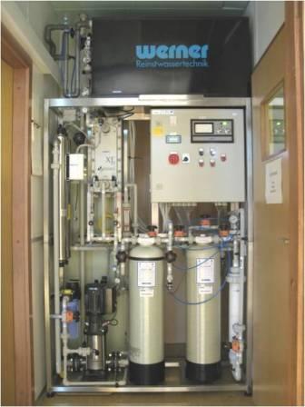
Semiconductor process technology and equipment available in LMSE allows investigations of basic physical phenomena and development of novel electronic devices, merging planar and MEMS specific technologies.

In the field of silicon planar technologies LMSE has over two decades of industrially proven experiences in design and fabrication of custom designed optical encoder silicon chips.

In the field of MEMS, LMSE is focusing on development of different structures and devices by integrating materials such as silicon, glass, PDMS, SU8, etc., for microfluidics with applications in medicine and bio-chemical engineering.

Clean room facilities
  • Location: LMSE, Faculty of Electrical Engineering UL, Ljubljana, Slovenia
  • Controlled parameters: temperature, humidity, airflow, particles
  • Class 100 (Federal Standard 209 E) i.e.. ISO class 5 (1999 ISO 14644-1), total area 70 m2
  • Class 10 under working bench flow booth, air ionizing equipment
  • Additional grey zone with background facilities (central vacuum system, central cleaning system, compressed air station, liquid nitrogen, central PPN system DI water)
Clean room
Grey zone