logo LMSE
Laboratory of Microsensor Structures and Electronics
faks_logo
Faculty of Electrical Engineering
Home
Activities
Physics & device modelling
Semiconductor & MEMS technologies
Photolithography
Diffusion & oxidation
Wet etching & wafer cleaning
Thin film deposition & etching
Material and device characterization
Electronics
Devices
Projects
Equipment ARRS
Members
Contact
Lectures

Valid HTML 4.01 Strict


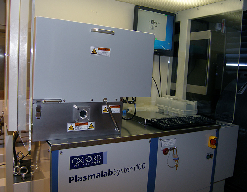
Deep Reactive Ion Etching
Plasmalab System 100 ICP 180
  • Inductive coupled plasma (ICP)
  • Lower (substrate) RF driven
  • Thermal contact by He backside cooling
  • Gas inlet through source and through distibution ring
Plasmalab 100
Plasmalab System 100

Technology
  • Bosch process - Si anisotropic etching
  • Resist removal
  • SiN, SiOx anisotropic etching

Gases
  • SF6
  • C4F8
  • Ar
  • O2
  • CHF3

PVD
PECVD
RIE
DRIE
Surface cleaning

uni_logo
University of Ljubljana